Directing the Enhancement of Efficiency in Silicon Device Design
Silicon stands as one of the predominant functional materials in contemporary society, serving as the foundational element for semiconductor technologies across a spectrum ranging from microelectronics to solar cells. Silicon transistors, crucial for computing applications spanning from cell phones to supercomputers, exemplify its pervasive impact.
Additionally, silicon photovoltaics represent the most extensively utilized solar-cell technology. According to the U.S. Department of Energy (DOE), nearly 50% of the new electric generation capacity in 2022 was attributed to solar cells, with silicon holding a 95% market share, as reported by the International Energy Agency (IEA). Despite silicon’s integral role in our modern lifestyle, numerous unresolved questions persist concerning its fundamental physical properties. In semiconductor devices, the functionality stems from the movement and interactions of subatomic particles, such as electrons (bearing negative charge) and holes (representing the absence of an electron from an otherwise occupied state, behaving like a positively charged particle).
These carriers facilitate the conveyance of electrical charge through the material. For instance, in a solar cell, the material absorbs incoming light, and the absorbed energy transforms into pairs of electrons and holes. Subsequently, these energized electrons and holes migrate to opposite ends of the solar cell, generating electricity. Regrettably, undesirable interactions between electrons and holes can occur, leading to the conversion of their energy into heat and restricting device efficiency. One notable loss mechanism involves carriers recombining and converting their energy into heat by interacting with defects in the material. Enhancing the quality of the material often proves effective in mitigating this defect-mediated recombination and improving overall device efficiency.

Certain interactions inherent to a material persist even in perfectly pure samples and cannot be eradicated. Auger-Meitner recombination (AMR), historically known as Auger recombination, falls into this category. Named after nuclear science pioneers Lise Meitner and Pierre Auger, who independently discovered this effect in atoms, the new nomenclature acknowledges Meitner’s contributions as she independently identified the process a year before Auger. In the semiconductor realm,
AMR involves the recombination of one electron and one hole, transferring their energy to a third carrier. This high-energy carrier can either thermalize or escape from a device, generating heat and diminishing energy-conversion efficiency or available carriers. Despite decades of research, the atomistic mechanisms of AMR in silicon have remained elusive. Dr. Kyle Bushick and Prof. Emmanouil Kioupakis from the University of Michigan’s Materials Science and Engineering have introduced a novel computational methodology.
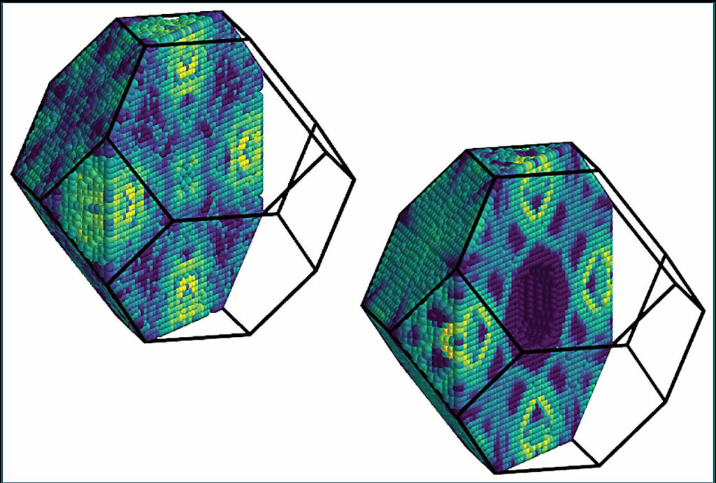
Utilizing supercomputing resources at the National Energy Research Scientific Computing Center (NERSC) of Lawrence Berkeley National Lab, they conducted comprehensive calculations of AMR in silicon, gaining atomic-level insights. The complexity of the AMR process in silicon arises from multiple permutations. The excited carrier can be an electron or a hole, leading to electron-electron-hole (eeh) and hole-hole-electron (hhe) processes, respectively. Moreover, AMR can be direct or phonon-assisted, where carriers interact with vibrating atoms (phonons) to transfer momentum.
Predictive atomistic calculations enable the direct computation and characterization of each component. The report, published in Physical Review Letters, emphasizes the significance of the phonon-assisted AMR process in silicon. The researchers demonstrate that electron-phonon interactions not only account for the entirety of the hhe process but also contribute significantly to the eeh process, resolving previous debates in the literature. They also propose a potential method for altering AMR in silicon through material strain.
This work provides a previously unavailable fundamental understanding of an intrinsic loss mechanism in the essential semiconductor silicon. The insights gained from this research can aid in designing more efficient devices by mitigating the impact of the undesirable AMR process, offering potential benefits to industries reliant on silicon devices like transistors and solar cells. Emmanouil Kioupakis, Associate Professor of Materials Science and Engineering at the University of Michigan, underscores the significance of this work in advancing our comprehension of losses in silicon devices and the potential for substantial benefits in industries such as transistors and solar cells.
This article is republished from PhysORG under a Creative Commons license. Read the original article.
Do not forget to share your opinion with us to provide you with the best posts !


0 Comments